Thermal imaging for PCB debugging enables non-invasive localization of sub-millimeter short circuits, power delivery network dropouts, and thermal impedance bottlenecks across high-density printed circuit board assemblies.
Deploying uncooled microbolometers with high thermal sensitivity (NETD < 40 mK) paired with dedicated macro-optics is mandatory to resolve microscopic 0201 and 01005 surface-mount passive faults down to 100 μm spot sizes without inducing thermal shock or leaving chemical residue.
Selecting between dedicated benchtop radiometric streaming instruments and cost-effective handheld platforms with clip-on optical elements dictates measurement repeatability, export compliance limits, and total laboratory cost of ownership.
Section 1: Physical Principles, Spatial Sampling, and Emissivity Calibration
Thermal diagnostics in microelectronics operate at the intersection of micro-scale heat transfer and infrared radiometry.
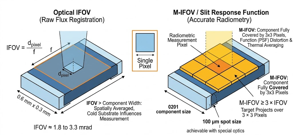
The spatial resolving capability of an uncooled microbolometer array is determined by its Instantaneous Field of View (IFOV = d_pixel / f, where d_pixel represents detector pixel pitch and f represents focal length) and its Measurement Instantaneous Field of View (M-IFOV).
While an optical IFOV registers raw radiant flux on an individual detector element, accurate quantitative radiometry requires a target to project across a minimum of 3 × 3 contiguous pixels (the M-IFOV / Slit Response Function) to avoid optical point spread function (PSF) distortion and background substrate thermal averaging.
Concurrently, Noise Equivalent Temperature Difference (NETD) defines the signal-to-noise threshold of the sensor array.
High-sensitivity detectors (NETD < 40 mK to < 35 mK) resolve localized micro-watt Joule heating (P_diss = I² × R_short) induced by low-current leakage paths (such as 50 mA traversing a cracked ceramic capacitor) without requiring excessive current injection that could alter failure mechanisms or induce silicon thermal runaway.
Accurate radiometric temperature calculation requires rigorous surface emissivity (ε) compensation across heterogeneous PCBA materials.
Unoxidized bare copper traces and ground planes exhibit extremely low emissivity (ε ≈ 0.03 to 0.07), acting as infrared mirrors that reflect ambient room temperatures and operator thermal signatures directly into the detector array.
Similarly, polished solder fillets (SAC305, SnPb) exhibit ε ≈ 0.05 to 0.15, causing an 85 °C joint to falsely register as barely 32 °C under uncalibrated inspection.
Conversely, matte solder masks (ε ≈ 0.88 to 0.94) and black epoxy semiconductor encapsulants (ε ≈ 0.90 to 0.95) provide stable, high-emissivity targets suitable for direct measurement.
To achieve repeatable quantification across mixed-material planes, engineers apply high-temperature polyimide (Kapton) tape (ε = 0.92), removable non-conductive matte chalk sprays (ε ≈ 0.96), or capture unpowered reference baseline frames (T_ambient) to execute differential thermal subtraction (ΔT = T_powered – T_ambient), effectively eliminating stationary ambient reflections.
| PCBA Material / Surface Type | Typical Emissivity Range (ε) | Radiometric Impact & Diagnostic Behavior | Mitigation & Standardization Protocol |
| Bare Copper Ground Pours & Traces | 0.03 – 0.07 | Specular reflection; reflects operator and camera chassis thermal signature. | Apply high-temperature polyimide tape or execute differential ΔT baseline subtraction. |
| Solder Fillets (SAC305, SnPb) | 0.05 – 0.15 | Extreme radiometric underreporting (e.g., registers ~32 °C at 85 °C actual). | Measure adjacent component terminal pad or apply removable matte chalk coating. |
| Matte Solder Mask (FR4 / Polyimide) | 0.88 – 0.94 | High radiant emission; minimal specular reflection; reliable direct reading. | Direct measurement with emissivity set to 0.90 in processing software suite. |
| Epoxy Encapsulation (QFN, BGA, SOIC) | 0.90 – 0.95 | Uniform thermal emission; ideal target for package junction-to-top (Ψ_JT) analysis. | Direct measurement with emissivity set to 0.92 to 0.94. |
| Polyimide (Kapton) Film Tape | 0.92 – 0.95 | Homogeneous high emissivity; stabilizes thermal gradients across reflective areas. | Applied directly over mixed copper/solder diagnostic test zones. |
| Removable Matte Chalk / Lacquer Spray | 0.95 – 0.97 | Establishes uniform radiometric surface without shifting thermal mass significantly. | Spray thin coat; clean with isopropyl alcohol (IPA) bath post-inspection. |
| Silicone / Acrylic Conformal Coating | 0.82 – 0.90 | High overall emissivity, but localized coating thickness variations create minor gradients. | Measure coated surfaces directly; account for thermal insulation lag during fast transients. |
| Ceramic Capacitor Bodies (Barium Titanate) | 0.80 – 0.88 | Moderately high emissivity on ceramic body, but metallic end caps exhibit low emissivity. | Focus cursor on central ceramic body rather than reflective metallized solder terminations. |
Section 2: Hardware Architecture and Comprehensive Comparison Matrix
Commercial thermal imaging architectures for electronic diagnostics diverge across handheld generalist instruments, fixed-stand benchtop systems, and modular sensor pods.
Sensor technology in modern platforms centers on uncooled Vanadium Oxide (VOx) or amorphous Silicon (a-Si) microbolometer focal plane arrays (FPAs) operating within the 7.5 to 14.0 μm long-wave infrared (LWIR) spectral band.
Native spatial resolutions range from 160 × 120 pixels in legacy units to 384 × 288 in enterprise systems. While multi-spectral visible edge fusion (such as FLIR MSX) enhances component identification by outlining silkscreen designators, it does not increase native radiometric pixel count.
Advanced platforms employ mathematical super-resolution reconstruction (such as Keysight Fine Resolution dither or HIKMICRO SuperIR) to synthesize higher spatial pixel densities from micro-dithered multi-frame captures, improving thermal edge clarity.
Frame rate parameters are strictly constrained by international dual-use export regulations, primarily the Wassenaar Arrangement and US Export Administration Regulations (EAR ECCN 6A003.b.4.b).
Cameras with refresh rates exceeding 9 Hz (such as 15 Hz, 25 Hz, 30 Hz, or 60 Hz) face international shipping and cross-border transfer controls, leading many general test instruments to operate at an unrestricted 9 Hz frequency.
While 9 Hz provides adequate fidelity for static DC thermal equilibrium profiling, dynamic transient impedance capture (Z_th), power rail startup current surges, and high-speed pulse-width modulation (PWM) load-step responses require 25 Hz to 30 Hz capture speeds to prevent lateral FR4 substrate thermal spreading from masking localized peak anomalies.
| Diagnostic Parameter | Teledyne FLIR E8 Pro | Teledyne FLIR ETS320 | Keysight U5855A TrueIR | HIKMICRO B20 / B20S | HIKMICRO Master M31 | Seek Thermal CompactPRO |
| Instrument Form Factor | Handheld Point-and-Shoot | Dedicated Benchtop Stand | Handheld Industrial | Handheld Modular | Handheld Industrial | Smartphone Modular Pod |
| Native IR Resolution | 320 × 240 (76,800 px) | 320 × 240 (76,800 px) | 160 × 120 (19,200 px) | 256 × 192 (49,152 px) | 384 × 288 (110,592 px) | 320 × 240 (76,800 px) |
| Enhancement Engine | MSX Visible Edge Fusion | None (Pure Radiometric) | Fine Resolution (320 × 240) | SuperIR (640 × 480 Live) | SuperIR (768 × 576 Live) | None (Software Filter) |
| Detector Architecture | Uncooled VOx Bolometer | Uncooled a-Si/VOx Bolometer | Uncooled VOx Bolometer | 12 μm VOx Array | 12 μm VOx Array | 12 μm VOx Array |
| Spectral Range | 7.5 to 13.0 μm | 7.5 to 13.0 μm | 8.0 to 14.0 μm | 7.5 to 14.0 μm | 7.5 to 14.0 μm | 7.5 to 14.0 μm |
| Thermal Sensitivity (NETD) | < 50 mK (0.05 °C) | < 60 mK (0.06 °C) | < 70 mK (0.07 °C) | < 40 mK (0.04 °C) | < 35 mK (0.035 °C) | < 70 mK (0.07 °C) |
| Refresh Frame Rate | 9 Hz (Unrestricted) | 9 Hz (Unrestricted) | 8 to 9 Hz (Unrestricted) | 25 Hz (Smooth Video) | 30 Hz (Smooth Video) | 15 Hz (FastFrame) |
| Field of View (FOV) | 33° × 25° (F/1.4) | 45° × 34° (F/1.5) | 28° × 21° (F/1.3) | 37.2° × 50.0° (F/1.0) | 41.1° × 30.5° (F/1.0) | 32° × 23° (Chalcogenide) |
| Min. Focus Distance | 0.36 m (Fixed Focus) | 70 mm ± 10 mm (Fixed) | 0.10 m (Manual Focus) | 0.30 m (Focus Free) | 0.10 m (Manual Focus) | 0.15 m (Manual Ring) |
| Macro Capabilities | No macro; ~1.8 mrad IFOV | Built-in: 170 μm spot @ 70 mm | Direct focus down to 10 cm | HM-B201: 100 μm target @ 30 mm | Native 10 cm; optional macro | ZnSe aftermarket optics |
| Video Telemetry | UVC Screen Cast (Non-Rad) | Full Radiometric USB Stream | Radiometric Log (8 fps SCPI) | UVC Screen Cast (Non-Rad) | Full Radiometric USB/Wi-Fi | Mobile Screen Stream |
| Software Suite | Thermal Studio / Ignite | FLIR Tools+ / Thermal Studio | TrueIR Analysis & Reporting | HIKMICRO Analyzer / App | HIKMICRO Studio Suite | Seek Mobile App / SDK |
| Measurement Accuracy | ±2 °C or ±2% of reading | ±3 °C or ±3% of reading | ±2 °C or ±2% of reading | ±2 °C or ±2% of reading | ±2 °C or ±2% of reading | ±5 °C or ±5% of reading |
| Commercial MSRP (2026) | $3,299.00 to $3,699.00 | $2,849.00 to $3,960.00 (EOL) | Discontinued ($3,800 List) | $399.00 to $549.00 (Lens: $89) | $3,500.00 to $3,850.00 | $499.00 to $599.00 |
| Secondary Valuation | $2,200.00 to $2,700.00 | $1,200.00 to $1,800.00 | $950.00 to $1,400.00 | $300.00 to $420.00 | $2,400.00 to $2,900.00 | $250.00 to $350.00 |
Section 3: Micro-Component Macro Diagnostics and Short-Circuit Localization
Locating microscopic low-impedance short circuits on high-density power delivery networks (such as VDD_CORE, VDD_DRAM, and VDD_IO) populated with dozens of parallel multilayer ceramic capacitors (MLCCs) presents acute spatial and thermal challenges.
As passive components scale down to 0201 (0.6 mm × 0.3 mm) and 01005 (0.4 mm × 0.2 mm) footprints, standard fixed-focus thermal cameras (IFOV ≈ 1.8 to 3.3 mrad at 0.3 m working distance) project a single-pixel footprint between 0.6 mm and 1.0 mm. At this coarse sampling ratio, an 0201 component cannot cover the required 3 × 3 pixel M-IFOV, causing the recorded temperature to be spatially averaged across the cold substrate and underestimating true hotspot temperatures by 40% to 70%.
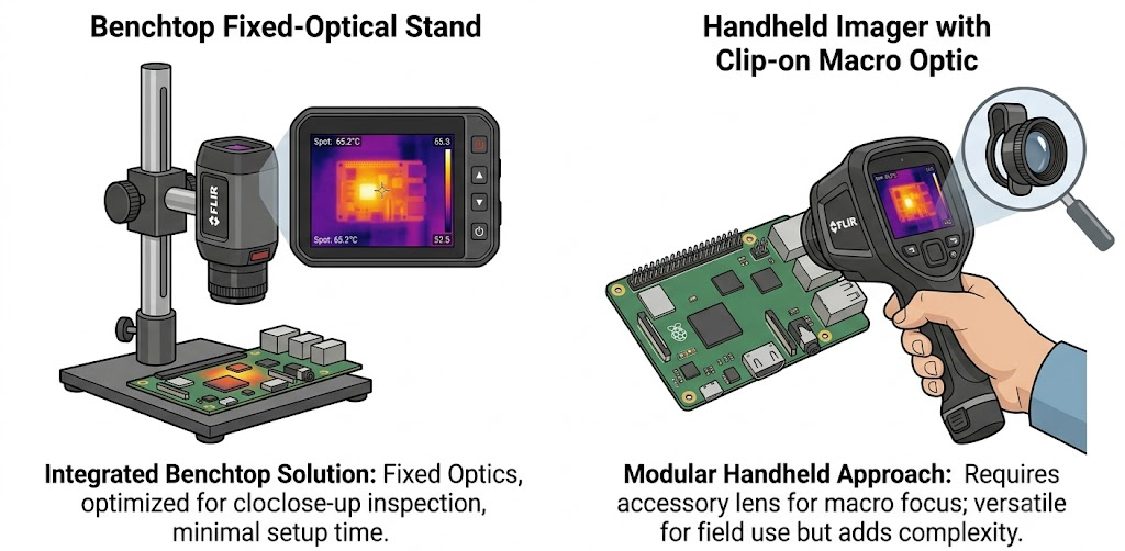
Deploying specialized optical configurations—such as the FLIR ETS320 (170 μm spot size at 70 mm working distance) or the HIKMICRO B20S equipped with an HM-B201-MACRO lens (100 μm resolving limit at 30 mm working distance)—is necessary to map thermal gradients directly across the component body versus its solder termination fillets.
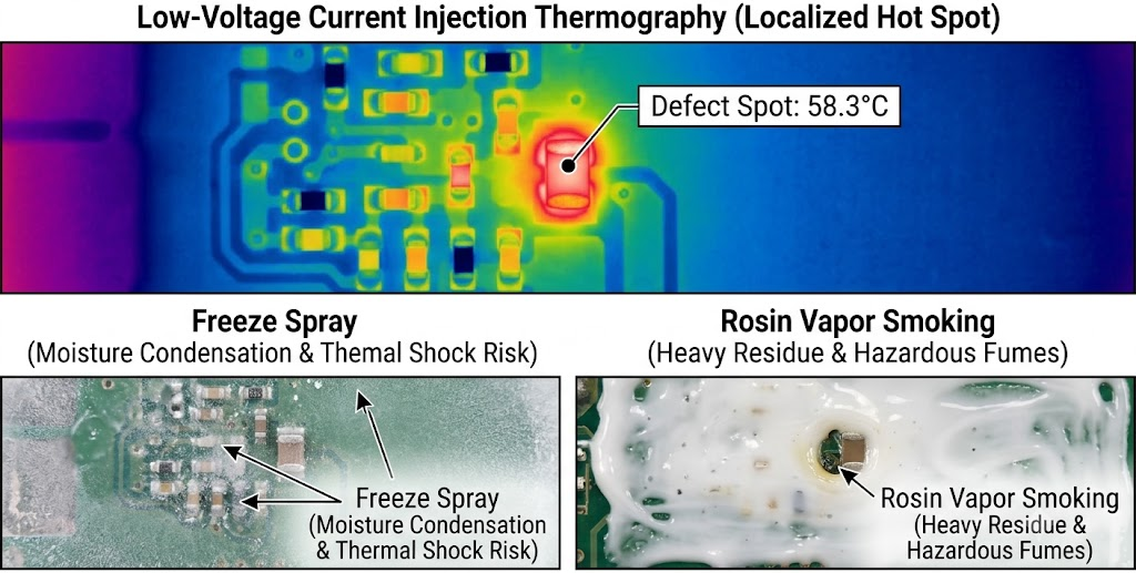
Low-voltage current injection thermography operates as an entirely non-invasive, residue-free diagnostic methodology. A benchtop DC power supply is configured to a non-destructive voltage clamp (0.5 V to 0.8 V for sub-1V core rails, or 1.0 V for 3.3 V/5 V rails) to avoid forward-biasing internal semiconductor ESD protection diodes or damaging unpowered silicon cores.
Current is injected starting at 50 mA and incremented gradually. Because shorted ceramic dielectrics or micro-solder bridges maintain localized residual resistance (R ≈ 0.05 Ω to 2.0 Ω), current concentrates at the defect point, producing measurable I²R power dissipation. A thermal imager with an NETD < 40 mK isolates the defect within seconds.
Conversely, legacy diagnostic techniques exhibit severe practical trade-offs. Freeze spray introduces severe thermal shock risks that crack ceramic MLCC dielectrics and produces moisture condensation that creates secondary conductive leakage paths. Rosin vapor smoking leaves sticky resin requiring chemical ultrasonic cleaning with toxic solvents. Isopropyl alcohol (IPA) evaporation requires excessive power dissipation (> 1 W to 5 W) that risks delaminating fine-pitch PCB copper traces before localized boiling becomes visible.
| Diagnostic Methodology | Sensitivity Floor | Board Residue & Physical Impact | Spatial Localization Precision | Physical Diagnostic Mechanism |
| Low-Voltage Current Injection Thermography | High (< 50 mW power dissipation) | Zero residue; fully non-destructive and non-contact. | Pinpoint sub-millimeter (optical/macro spot dependent). | Direct microbolometer detection of localized Joule heating (I²R). |
| Freeze Spray (Aerosol Rapid Coolant) | Moderate (~200 mW power dissipation) | Liquid condensation; thermal shock risk to MLCCs/silicon. | Moderate (blurred thermal melting perimeter). | Rapid solid-to-liquid phase transition of condensed frost layer. |
| Rosin / Flux Vapor Smoking | High (~100 mW power dissipation) | Heavy sticky rosin residue; emits hazardous fumes. | High (sharp optical melting transition at ~60 °C). | Solid-to-liquid phase change turning opaque white film transparent. |
| Isopropyl Alcohol (IPA) Evaporation | Low (> 1000 mW power dissipation) | Zero residue; volatile fluid evaporates completely. | Low (liquid pooling and surface tension spreading). | Convective mass transfer and boiling/evaporation under high heat. |
Section 4: Software Ecosystems, Dynamic Radiometric Streaming, and Data Integrity
Failure analysis and reliability engineering require continuous, multi-point temperature-over-time telemetry to characterize thermal impedance parameters (junction-to-ambient R_θJA, junction-to-top Ψ_JT) and evaluate power stage transient behaviors.
A fundamental operational distinction exists between instruments supporting true radiometric video streaming versus standard uncompressed screen casting (UVC):
- True Dynamic Radiometric Video Streaming (e.g., FLIR ETS320, HIKMICRO Master M31, Keysight U5855A): The imager continuously transmits raw 14-bit analog-to-digital converter (ADC) microbolometer data frame-by-frame over USB or Wi-Fi to host analysis software.
- This raw telemetry allows test engineers to retrospectively reposition spot meters, draw new area profiles, alter emissivity values, adjust background temperature reflections, and recalculate absolute temperature arrays across every recorded frame after the physical test run concludes.
- UVC / Screen-Mirrored Video Streaming (e.g., FLIR E8 Pro, HIKMICRO B20S): The imager’s internal signal processor applies color palette quantization, temperature spans, and graphic overlays locally, streaming an 8-bit YUV/RGB video feed over USB.
- PC-side software functions strictly as a display monitor; absolute per-pixel radiometric data cannot be recalculated or re-calibrated retrospectively once streaming concludes.
Desktop analysis suites provide advanced post-capture processing capabilities.
The Teledyne FLIR Thermal Studio ecosystem supports multi-palette isotherm segmentation, formula-driven batch quantification, and embedding of 14-bit radiometric matrices directly within standard JPEG metadata containers.
The HIKMICRO Analyzer and Studio platforms provide real-time USB recording, 3D thermal surface topography mapping, and per-pixel Kelvin export into radiometric BMP/JPEG formats without recurring licensing fees.
The Keysight TrueIR Analysis & Reporting Tool provides direct SCPI automation interfacing, virtual instrument logging, and multi-point delta-T trending profiles for automated test bench environments.
| Software Telemetry Feature | Teledyne FLIR Thermal Studio / Ignite | HIKMICRO Analyzer / Studio Suite | Keysight TrueIR Analysis Tool | Seek Thermal Mobile / SDK |
| Native Radiometric File Format | 14-bit Radiometric JPEG Container | Radiometric BMP / JPEG (Raw Kelvin) | Proprietary Radiometric Data / SCPI | Proprietary Mobile Container / TIFF |
| Dynamic Video Re-calibration | Supported (Full per-pixel post-processing) | Supported on Master/M-Series platforms | Supported via 8 fps PC logging mode | Unsupported (Fixed rendering) |
| Multi-Point Transient ΔT Logging | Advanced automated formula graphing | Real-time USB plot generation & 3D maps | Automated SCPI-driven multi-spot logs | Basic mobile point temperature readout |
| Cloud Synchronization & Enterprise | FLIR Ignite direct Wi-Fi sync | Local network / manual cloud export | Local enterprise database export | Direct smartphone storage sync |
| Licensing Model | Tiered Subscription / Perpetual License | Free Lifetime License (No recurring cost) | Perpetual License (Included with HW) | Free Mobile App / Developer SDK |
Section 5: Strategic Procurement, Secondary Market Valuation, and TCO Decision Matrix
Engineering procurement decisions must balance capital expenditure (CapEx), optical adaptability, software licensing, and product lifecycle support.
The Teledyne FLIR ETS320 remains an industry benchmark for benchtop electronics diagnostics due to its integrated microscope stand and full radiometric USB streaming.
However, because Teledyne FLIR classified the ETS320 as End-of-Life (EOL), distributor inventory is exhausted, driving procurement into secondary liquidator channels where refurbished units command between $1,200.00 and $1,800.00. The Keysight U5855A TrueIR trades on surplus markets between $950.00 and $1,400.00, retained primarily by laboratories requiring legacy SCPI test bench automation.
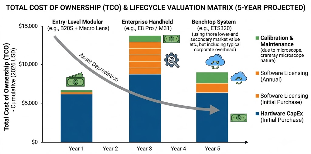
For modern lab outfitting, modular platforms offer exceptional performance-to-cost ratios.
The HIKMICRO B20/B20S platform ($399.00 to $549.00 MSRP) paired with the HM-B201-MACRO clip-on lens ($89.00 to $120.00) delivers 256 × 192 native resolution, 25 Hz refresh rate, < 40 mK NETD, and 100 μm optical resolving limits for under $650.00 total CapEx.
For enterprise compliance, high-volume production, or building-level predictive maintenance, the FLIR E8 Pro ($3,299.00 to $3,699.00) and HIKMICRO Master M31 ($3,500.00 to $3,850.00) provide ruggedized drop-tested enclosures, higher native resolutions, and comprehensive enterprise cloud ecosystems.
When assessing short-term projects versus permanent laboratory infrastructure, the Buy versus Rent decision hinges on utilization duty cycles and calibration overhead.
Renting high-end radiometric thermal analyzers ($800.00 to $1,500.00 per month) is strategically advantageous for specialized New Product Introduction (NPI) qualification runs or compliance audits requiring certified annual NIST calibration certificates without incurring long-term depreciation.
Conversely, purchasing modular units (such as the B20S or secondary ETS320) achieves full capital amortization within two to three diagnostic cycles by eliminating third-party failure analysis turnaround delays.
| Engineering Application Profile | Recommended Solution | Strategic Justification | Key Operational Constraints |
| Laboratory R&D & Continuous Power Integrity Logging | Teledyne FLIR ETS320 (Secondary) or HIKMICRO M31 + Rig | Hands-free stand, 170 μm spot size at 70 mm working distance, full dynamic USB radiometric streaming into PC software. | ETS320 is factory EOL; 9 Hz frame rate limit on FLIR units. |
| High-Density Board Repair & Short-Circuit Hunting | HIKMICRO B20S + HM-B201-MACRO Lens | 100 μm optical resolving limit at 30 mm working distance, < 40 mK NETD, 25 Hz refresh rate, low total cost of ownership. | Fixed 30 mm macro working distance limits clearance for tall physical oscilloscope probes. |
| Enterprise Facility Audits & Electrical Panel QA | Teledyne FLIR E8 Pro | Rugged drop-tested housing, MSX edge overlay, direct Wi-Fi sync to FLIR Ignite Cloud and corporate reporting tools. | Fixed 0.36 m minimum focus distance makes macro SMD PCB inspection impossible without external mods. |
| Field Service Triage & Ultra-Low-Budget Diagnostics | Seek Thermal CompactPRO + ZnSe Macro Lens | Ultra-compact form factor, native 320 × 240 sensor, adaptable via aftermarket laser ZnSe meniscus lenses. | High noise floor (NETD < 70 mK), no dynamic PC radiometric video streaming, smartphone battery thermal drift. |
Related Engineering & Metrology Guides:
- Pre-Layout Thermal Simulation: Catch thermal hotspots before fabrication by integrating cloud-native FEA solvers—explore our analysis on [Enterprise Cloud EDA: Altium 365 vs. Ansys Cloud Integration].
- Precision Voltage & Shunt Diagnostics: For measuring microvolt drops and low-resistance shorts alongside thermal scans, explore our [Metrological Analysis of 6.5-Digit Bench Multimeters].
Section 6: Source Directory and Standardized Regulatory Notice
Commercial Documentation and Distributor Directory
- Teledyne FLIR E8 Pro Official Datasheet: https://flir.netx.net/file/asset/58068/original/attachment
- Teledyne FLIR E8 Pro Mouser Listing: https://www.mouser.com/en/c/?m=Teledyne%20FLIR
- Teledyne FLIR ETS320 Product Specification: https://www.flir.com/products/ets320/
- Teledyne FLIR ETS320 Technical Archive: https://www.flir.com/ko-kr/products/ets320/
- HIKMICRO B20 / B20S Industrial Datasheet: https://webassets.hikmicrotech.com/global/asset/95d71515037347dfa72a6903f525c7c9.pdf
- HIKMICRO B Series Macro Lens Specification: https://www.hikmicrotech.com/en/industrial-products/b-series-macro-lens/
- HIKMICRO Master M31 Datasheet: https://webassets.hikmicrotech.com/global/asset/d5290f17904e4e278c2a283bf8d350d3.pdf
- Keysight U5855A TrueIR Technical Overview: https://www.keysight.com/us/en/product/U5855A/trueir-thermal-imager-350-c.html
- Seek Thermal CompactPRO Product Profile:
https://www.thermal.com/compact-series-cameras.html
Standardized 2026 Regulatory and Compliance Notice
Thermal imaging systems operating with frame refresh rates exceeding 9 Hz (including 15 Hz, 25 Hz, 30 Hz, and 60 Hz configurations) are subject to international export control regulations under the Wassenaar Arrangement (Dual-Use List Category 6) and the United States Department of Commerce Export Administration Regulations (EAR, 15 CFR Part 774, ECCN 6A003.b.4.b).
Re-exportation, transshipment, or diversion contrary to applicable United States, European Union, or national laws without official authorization licenses is strictly prohibited.
Radiometric accuracy figures (±2 °C or ±2%) require annual factory calibration traceable to national metrology institutes (NIST/DKD) and valid atmospheric/emissivity parameter configurations.
Technical parameters, secondary market valuations, and distributor catalog listings reflect validated market conditions as of 2026.
2 thoughts on “Thermal Imaging for PCB Debugging and Power Integrity: 2026 Engineering Guide”