Executive Summary
Modern embedded firmware and hardware protocol validation relies on three core logic analyzer architectures:
- Host-Streaming USB Logic Analyzers (e.g., Saleae Logic Pro series): Stream multi-gigabyte trace records directly over high-throughput USB 3.0 links into host PC RAM for continuous, multi-hour transaction recording.
- FPGA-Buffered Systems (e.g., Digilent Digital Discovery): Isolate signal capture into dedicated local DDR3/SRAM to eliminate operating system transfer latency, ensuring deterministic, lossless capture during high-frequency burst events.
- All-in-One Multi-Function Debuggers (e.g., Digilent Analog Discovery 3): Integrate digital logic analysis with analog oscilloscope channels and waveform generators for versatile, budget-conscious benchtop validation.
Selecting the right platform requires balancing continuous transaction depth, low input capacitance loading (Cin < 10 pF), sub-1.8V low-voltage logic threshold support, and automated continuous integration (CI) scripting capabilities.
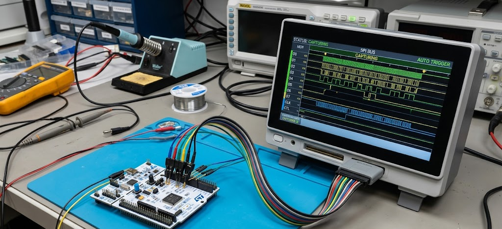
1. Logic Analyzer Architectures: Streaming USB vs. On-Board Hardware Buffering
Host-Streaming USB Architecture (e.g., Saleae Logic Pro)
Host-streaming logic analyzers route digitized signals directly from high-speed front-end comparators through a physical USB 3.0 controller into host PC memory (RAM).
- Primary Advantage: Continuous, multi-hour protocol captures bounded only by host storage and RAM capacity. Essential for diagnosing intermittent firmware lockups, tracing deep RTOS task switches, and tracking long power-up sequences.
- Hardware Bottleneck: Relies entirely on the host operating system’s USB stack, xHCI driver scheduling, CPU frequency scaling, and Direct Memory Access (DMA) channel availability.
- Failure Mode: Under sustained high bandwidth, host-side interrupt latency can cause small internal First-In, First-Out (FIFO) buffers to overflow, resulting in dropped packets and unrecoverable acquisition gaps.
On-Board Hardware Buffering (e.g., Digilent Digital Discovery)
On-board buffered instruments decouple data acquisition from the host transfer pipeline by routing signals directly into dedicated Field Programmable Gate Array (FPGA) logic paired with local high-speed memory (SRAM or DDR3 SDRAM).
- Primary Advantage: Guarantees deterministic, 100% lossless signal acquisition at peak sampling rates (e.g., up to 800 MS/s) regardless of host CPU load or OS scheduling delays.
- Hardware Trade-Off: Total capture duration is strictly limited by the physical capacity of the local buffer (e.g., 2 Gbit DDR3).
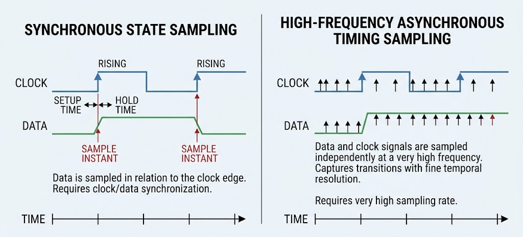
Synchronous State vs. Asynchronous Timing Analysis
Digital validation requires choosing between two primary capture methods:
- Synchronous State Analysis:
- Uses an external clock line supplied directly by the Device Under Test (DUT).
- Samples data strictly on active clock transitions, mirroring the setup and hold characteristics of synchronous digital receivers.
- Maximizes memory efficiency by recording data only during valid bus transitions, enabling compact buffers to store thousands of bus frames across SPI or parallel buses.
- Asynchronous Timing Analysis:
- Utilizes an internal high-stability crystal oscillator to sample inputs at uniform, high-speed time intervals independent of the target system clock.
- Detecting timing anomalies—such as setup/hold violations, clock jitter, race conditions, and narrow glitch pulses—requires significant oversampling.
- Rule of Thumb: A standard Nyquist rate (2x) is insufficient for pulse reconstruction; reliable edge placement requires a 4x to 5x oversampling factor, with 10x oversampling recommended for sub-nanosecond resolution.
- Example: Validating a 50 MHz SPI bus requires an asynchronous sample rate of at least 250 MS/s to 500 MS/s.
Key Takeaway: Choose Host-Streaming for deep, software-level protocol debugging over hours; choose FPGA-Buffered systems when zero-loss signal integrity during ultra-fast hardware bursts is mandatory.
2. Technical Benchmark Matrix (2026 Industry Standards)
| Model | Architecture Class | Digital / Analog Ch | Max Sample Rate (Digital / Analog) | Logic Threshold Range | Memory / Buffer Depth | 2026 MSRP (USD) | Sourcing & Specs |
| Saleae Logic Pro 16 | USB 3.0 Host-Streaming / MSO | 16 Ch / 16 Ch | 500 MS/s (4 Ch) / 50 MS/s | Selectable (0.6V, 0.9V, 1.65V) | Host RAM Limited (10B+ Samples) | $1,499.00 | View Product Page |
| Digilent Digital Discovery | High-Speed FPGA Buffer / USB 2.0 | 32 Ch (HS Probe) / 0 Ch | 800 MS/s (8 Ch) / N/A | Variable (1.2V to 3.3V CMOS) | 2 Gbit Local DDR3 SDRAM | $401.50 | View Product Page |
| Digilent Analog Discovery 3 | Multi-Function MSO / USB 2.0 | 16 Ch / 2 Ch | 125 MS/s / 125 MS/s | Fixed 3.3V (5.0V Tolerant) | Local FPGA Buffer + Stream | $379.00 – $450.00 | View Product Page |
| DreamSourceLab DSLogic U3Pro16 | Dual-Mode USB 3.0 / FPGA Buffer | 16 Ch / 0 Ch | 1.0 GS/s (4 Ch) / N/A | Continuously Variable (0.0V – 5.0V) | 2 Gbit DDR3 / 16G SuperStream | $299.00 | View Product Page |
| Intronix Logicport LA1034 | Compact FPGA Buffer / USB 2.0 | 34 Ch / 0 Ch | 500 MS/s (All Ch) / N/A | Continuously Variable (0.0V – 5.0V) | 34 x 2048 Static SRAM + RLE | Legacy ($150 – $250) | View Product Page |
3. Signal Integrity, Input Loading, and High-Speed Bus Decoding
Parasitic Probe Loading Model
Attaching a logic analyzer probe to a high-speed circuit introduces physical load impedances that can alter target behavior:
- Shunt Input Resistance (Rin): Typically 100 kΩ to 2 MΩ. High enough to prevent DC loading and quiescent current draw.
- Parasitic Capacitance (Cin): Ranges between 10 pF and 20 pF. In combination with the DUT driver output impedance, this creates a low-pass RC filter.
- Lead Inductance (Llead): Approximately 1 nH per millimeter of flying lead wire. Long ground wires create large return loops, inducing ground bounce, ringing, and false edge crossings.
Signal Integrity Impact on High-Speed Protocols
- High-Speed SPI (50+ MHz) & CAN-FD (5 Mbps data phase): Excess probe capacitance rounds active clock edges, erodes setup/hold margins, and can cause a previously functional circuit to fail while under test.
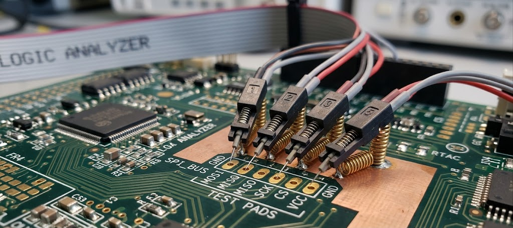
- Mitigation Best Practices: Use sub-10 pF active/passive probes, short ground spring clips instead of long flying leads, and series damping resistors (50 Ω to 100 Ω) placed near the test point.
Low-Voltage Logic Thresholds (1.2V / 1.8V)
Modern ultra-low-power microcontrollers and FPGAs operate on 1.2V, 1.5V, or 1.8V I/O rails.
- The Problem with Fixed Thresholds: A fixed 1.65V or 3.3V threshold comparator will fail to detect high states on 1.2V logic rails or will misinterpret ground rail noise as valid transitions.
- The Solution: Instruments with continuously adjustable or low-voltage selectable comparators allow engineers to set the slice voltage precisely at the 50% transition level (0.6V threshold for 1.2V logic), maintaining duty cycle fidelity and reliable packet framing.
Key Takeaway: Fast clock edges (> 50 MHz) require Logic analyzers with Cin < 10 pF input capacitance and user-adjustable input thresholds to validate sub-1.8V low-power buses without false-trigger artifacts.
4. Software Ecosystems, Protocol Filtering, and Automation APIs
Visual Debugging & Mixed-Signal Correlation
Modern analysis suites (Saleae Logic 2, Digilent WaveForms, DreamSourceLab DSView) convert gigabytes of raw binary transitions into structured protocol packets:
- Multi-Layer Filtering: Search millions of frames for specific errors (such as I2C NACKs, SPI framing violations, or CAN-FD CRC errors) without manual trace inspection.
- Mixed-Signal Correlation: Align digital protocol decodes with synchronized analog traces on the exact same time base. This enables instant diagnosis of whether a corrupted packet was caused by a firmware bug or a physical-layer defect (such as power rail droop, line ringing, or slow rise-times).
CI/CD Pipeline Automation & Scripting
Modern hardware-in-the-loop (HIL) test setups integrate logic analyzers directly into continuous integration pipelines using Python, C++, or gRPC/REST APIs:
- Automated Regression Testing: Configure triggers, execute DUT test suites, and extract decoded protocol payloads programmatically.
- Packet Error Rate (PER) Tracking: Monitor communications stability across extended thermal and voltage stress cycles.
- Continuous Compliance: Identify timing regressions and bus contention issues before hardware reaches mass production.
Key Takeaway: Advanced analysis software reduces debug cycles by correlating physical-layer analog anomalies with higher-level protocol errors, while Python and gRPC APIs enable fully automated HIL validation.
5. Strategic Sourcing, Total Cost of Ownership (TCO), and Verdict
Procurement Tiers
- Premium Professional Tier ($1,000 – $2,500): Best for full-time embedded firmware, hardware validation, and SoC development teams requiring minimal setup friction, regular API updates, and high-bandwidth mixed-signal capabilities.
- Mid-Tier Multi-Instrument ($350 – $500): Ideal for hardware labs, test engineers, and distributed teams needing high-speed FPGA state analysis, pattern generation, and oscilloscopes in a compact USB unit.
- Entry-Level / Maker Tier ($150 – $300): Suitable for individual developers, students, and budget-conscious repair benches needing high-channel digital debugging at minimal capital outlay.
Final Verdict & Sourcing Recommendations
- Best for Embedded Firmware & Mixed-Signal Debugging:
Saleae Logic Pro 16
The industry gold standard for day-to-day firmware and SoC development. Offers seamless UI navigation, multi-hour USB 3.0 streaming, and synchronized analog channel correlation.
👉 Check Saleae Logic Pro 16 Specifications & Pricing - Best for High-Speed FPGA & Digital State Analysis:
Digilent Digital Discovery
The top choice for pure digital validation. Delivers 800 MS/s sampling rates, dedicated 2 Gbit FPGA buffering, and 32 channels at an accessible price point.
👉 Check Digilent Digital Discovery Availability - Best All-In-One Laboratory Multi-Tool:
Digilent Analog Discovery 3
The most versatile diagnostic instrument for general-purpose electronics benches, combining a 16-channel logic analyzer, 2-channel oscilloscope, and arbitrary waveform generator.
👉 Check Digilent Analog Discovery 3 Options
6. Technical Manuals and Official References
- Saleae Logic Pro Hardware Specifications: Saleae Documentation
- Digilent Digital Discovery Reference Manual: Digilent Resource Center
- Digilent Analog Discovery 3 Technical Reference: Digilent Reference Portal
- Intronix Logicport LA1034 Specifications: PC Test Instruments Manuals
- DreamSourceLab DSLogic Series Documentation: DreamSourceLab Resources
7. Legal Disclaimer
All technical specifications, sampling rates, memory depths, protocol decoder listings, and MSRP pricing reflect manufacturer documentation as of 2026 and are subject to change without notice. Engineers should verify specific operating parameters, logic threshold ranges, and driver compatibility directly with respective equipment manufacturers prior to system integration.